
As the signal rise time decreases and the signal frequency increases, the EMI problem of electronic products is more and more concerned by electronic engineers. Almost 60% of EMI problems can be solved by high-speed PCB. Here are the nine rules:
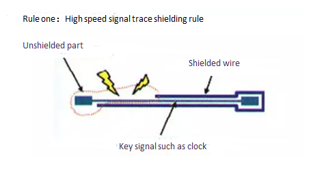
In high-speed PCB design, critical high-speed signal lines such as clocks need to be shielded. If there is no shielding or only part of the shielding, it will cause EMI leakage. It is recommended to shield the wire, every 1000 mil, punch the ground.
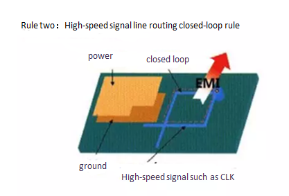
Due to the increasing density of PCB boards, many PCB LAYOUT engineers are prone to a mistake in the process of routing, that is, high-speed signal networks such as clock signals, which produce closed-loop results when multi-layer PCBs are routed. Such a closed loop result will produce a loop antenna that increases the radiant intensity of EMI.
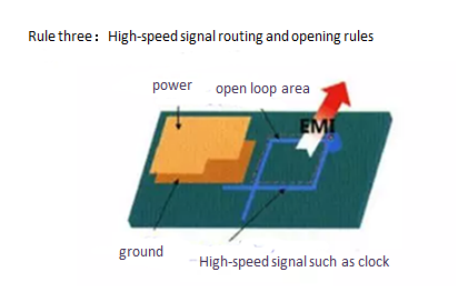
Rule 2 mentions that the closed loop of a high speed signal will cause EMI radiation, however open loop will also cause EMI radiation. A high-speed signal network, such as a clock signal, produces a linear antenna that increases the radiant intensity of EMI once it has an open loop result in a multi-layer PCB trace.
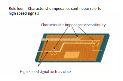
For high-speed signals, the continuity of the characteristic impedance must be ensured when switching between layers. Otherwise, EMI radiation will increase. That is to say, the width of the wiring of the same layer must be continuous, and the trace impedance of different layers must be continuous.
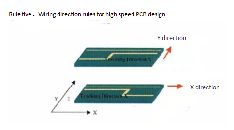
The traces between adjacent two layers must follow the principle of vertical traces, otherwise crosstalk between lines will be caused, and EMI radiation will be increased.
In short, the adjacent wiring layers follow the horizontal and vertical wiring directions, and the vertical wiring can suppress crosstalk between lines.
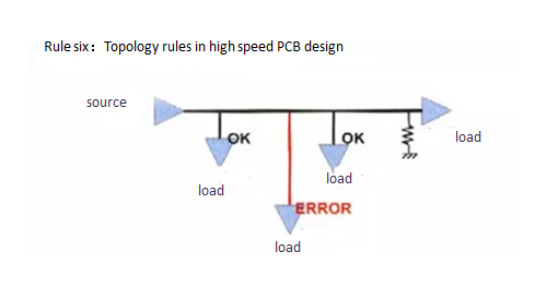
In high-speed PCB design, the control of the characteristic impedance of the circuit board and the design of the topology under multi-load conditions directly determine the success or failure of the product.
The illustration shows a daisy chain topology, which is generally used in the case of several Mhz. A star-shaped symmetrical structure at the back end is recommended for high-speed PCB design.
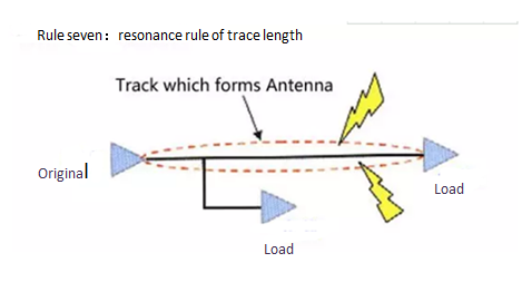
Check that the length of the signal line and the frequency of the signal constitute resonance, that is, when the wiring length is an integral multiple of the signal wavelength 1/4, the wiring will resonate, and the resonance will radiate electromagnetic waves, causing interference.
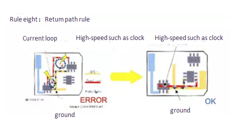
All high speed signals must have a good return path. As much as possible, ensure that the return path of high-speed signals such as clocks is minimized. Otherwise, the radiation is greatly increased, and the magnitude of the radiation is proportional to the area surrounded by the signal path and the return path.
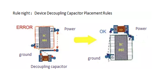
The placement of the decoupling capacitors is very important. Unreasonable placement does not result in decoupling. The principle is: close to the pin of the power supply, and the area enclosed by the power supply trace and ground of the capacitor is the smallest.